Happy Monday! Here’s what’s inside this week’s newsletter:
Deep dive: Breaking the Memory Wall Pt. 3 focuses on manufacturing constraints in advanced memory, showing how metrology, inspection limits, and buried defects now gate further scaling of 3D NAND.
Spotlights: Unconventional AI raises a $475M seed round to explore biologically inspired analog computing, while Nvidia-backed Starcloud trains an AI model in orbit, highlighting new directions in compute deployment.
Headlines: Updates across semiconductors and edge AI, continued momentum in quantum and photonics, advances in neuromorphic hardware, expanding data center infrastructure, and new developments in cloud, networking, and AI.
Readings: Record semiconductor revenues, advances in quantum photonics and diamond-based devices, real-time neuromorphic processors, liquid-cooled data centers, and the growing role of industrial and data cloud infrastructure.
Funding news: A compact set of rounds spanning quantum, neuromorphic computing, semiconductors, and data centers, with deal sizes ranging from €2M to $475M and no clear concentration in a single category.
Bonus: Technologies unveiled at IEDM 2025 highlight progress in HBM thermals, monolithic 3D integration, compute-in-memory devices, advanced lithography, silicon photonics, and automotive AI processors.
Deep Dive: Breaking the Memory Wall Pt. 3 – Metrology as a Prerequisite for Scaling Memory
3D NAND scales by stacking memory cells vertically
For more than a decade, 3D NAND (the dominant non-volatile memory technology used in solid-state drives across data centers, PCs, and mobile devices) has scaled by adding more layers on top of each other. Each new generation increases bit density by roughly 30%, with current chips reaching terabit-scale capacity per die.
From the outside, this looks like a straightforward continuation of vertical scaling. While patterning and deposition are challenging, the ability to measure and verify deep, buried structures also increasingly limits how aggressively 3D NAND can scale.
As stacks grow taller, precision becomes more critical
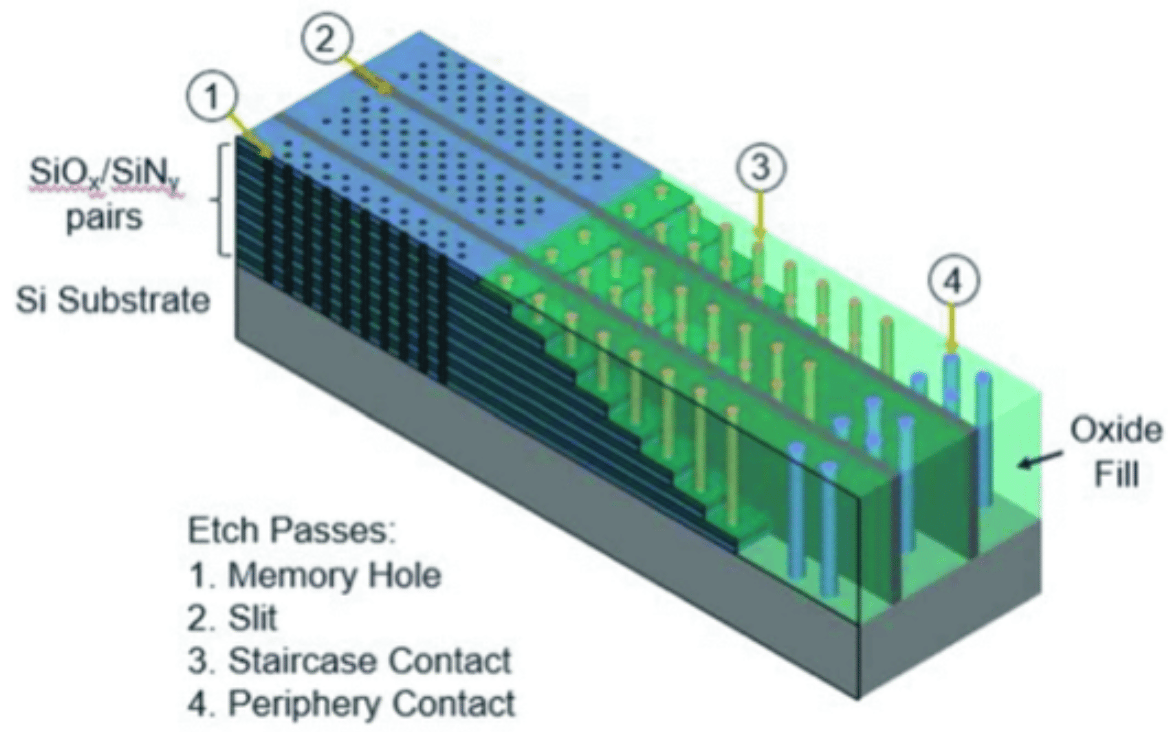
Modern 3D NAND relies on drilling extremely narrow vertical holes through stacks that can be several microns tall. These holes are well below 100 nm in diameter and must remain almost perfectly vertical from top to bottom. Any bowing, tapering, or misalignment can cause electrical interference between cells, making higher-density storage modes like QLC and PLC (quad-level cell and penta-level cell NAND, where each memory cell stores four or five bits by using multiple voltage levels) unreliable.
Most yield-critical defects are buried inside the memory stack
The challenge is that the most critical defects are buried. They occur inside the stack, not on the surface. Traditional inspection tools were designed to examine flat, easily accessible features. In 3D NAND, many yield-limiting defects sit several microns below the surface and cannot be detected with conventional electron-beam or atomic-force–based inspection techniques.
Metrology requires multiple, system-level inspection methods
As a result, metrology for 3D NAND has become a multi-modal problem. Manufacturers combine several complementary techniques, each compensating for the blind spots of the others:
Infrared optical metrology (IRCD) uses longer wavelengths of light that can penetrate deeper into stacked oxide and nitride layers, allowing indirect measurement of vertical feature profiles at high throughput.
High-energy electron-beam inspection uses higher landing energies so electrons can reach several microns into deep features and detect buried defects such as residual metal or voids.
X-ray inspection and X-ray CT allow non-destructive imaging of buried structures and alignment across tall stacks, where optical and electron-beam techniques struggle.
Acoustic microscopy is used after wafer bonding to detect voids or other bonding-related defects at the interface between the NAND memory array and the underlying logic die.
None of these tools alone is sufficient. Yield depends on correlating partial, indirect signals across multiple inspection methods.
Limited visibility increases reliance on virtual metrology
A second, less visible shift is the growing role of virtual metrology. Manufacturers increasingly rely on process simulation and virtual fabrication to predict where defects are likely to occur and to determine how aggressively real wafers need to be sampled. This helps reduce trial-and-error during development without replacing physical measurement.
Source: Metrology digs deep to produce next-generation 3D NAND (SemiEngineering)
Spotlights
“Barely two months after launch, Unconventional AI has secured a $475 million seed round at a valuation of $4.5 billion. The round was co-led by Andreessen Horowitz and Lightspeed Venture Partners, with participation from Lux Capital, DCVC, Databricks and Amazon founder Jeff Bezos.
[...]
Unconventional AI is exploring ideas rooted in biology, where energy is a scarce resource and efficiency is essential. The human brain, for example, performs extraordinary computation while consuming only about 20 watts, a far cry from today’s power-hungry AI systems.
The startup is investigating how biological principles and the analogue foundations of computing might translate into processors that harness the inherent physics of semiconductors rather than brute-force digital switching.”
💥 Nvidia-backed Starcloud trains first AI model in space as orbital data center race heats up (CNBC)
“Washington-based Starcloud launched a satellite with an Nvidia H100 graphics processing unit in early November, sending a chip into outer space that’s 100 times more powerful than any GPU compute that has been in space before.
Now, the company’s Starcloud-1 satellite is running and querying responses from Gemma, an open large language model from Google, in orbit.”
Read more about Starcloud in our recent interview!
Headlines
Last week’s headlines featured new semiconductor and edge AI hardware, momentum in quantum and photonics, advances in neuromorphic chips, expanding data center infrastructure, and updates across cloud, networking, and AI.
🦾 Semiconductors
China’s CSPs and OEMs likely to Actively Procure H200, but Domestic AI Chip Development Continues to Accelerate (TrendForce)
Advantest Introduces Next-Generation M5241 Memory Handler to Support High-Performance AI Memory Devices (Advantest)
Infineon extends the CoolSiC™ MOSFET 750 V G2 family featuring ultra-low RDS(on) and new packages (Infineon)
DEEPX Launches DX-H1 V-NPU: The 30W Single-Card Solution That Challenges GPU Dominance (PR Newswire)
⚛️ Quantum
Einride and IonQ partnership uses quantum computing to optimize the logistics of electric and autonomous freight (The Quantum Insider)
Google Opens Its Advanced Willow Chip to UK Researchers in Search For Practical Uses (The Quantum Insider)
MicroAlign Breakthrough: From 12 to 24-Channel High Accuracy Fiber Arrays for Quantum Photonic Computing (MicroAlign)
How Fujitsu Is Tackling a 10,000-Qubit Quantum Computer for Practical Applications (The Quantum Insider)
Quantum Corridor, Toshiba Demonstrate Cross-State Quantum Key Distribution Over Live Commercial Metro Fiber Network (The Quantum Insider)
⚡️ Photonics
Ayar Labs and yieldWerx Partner to Streamline Photonics Test Data Analytics, Delivering Measurable Results in Just 30 Days (PR Newswire)
Hamamatsu Photonics Develops “HyperGauge® In-plane Film Thickness Meter” Achieves Full-Surface Measurement of 300 mm Wafers in Just 5 Seconds (Hamamatsu Photonics)
PI launches NanoCube 6-axis piezo platform for photonics (Design World)
🧠 Neuromorphic
Lancaster spinout Quinas Technology launches ULTRARAM™ memory technology project with Innovate UK (Lancaster University)
Korea ranks second globally in neuromorphic chip patent growth (Communications Today)
💥 Data Centers
Siemens and nVent to release joint reference architecture purpose-built for NVIDIA AI data centers (Siemens)
Taiwan unveils national cloud center amid global AI race (Evrim Ağacı)
☁️ Cloud
PowerBank Announces Launch of the First Satellite in the “Orbital Cloud” Project with Smartlink AI (PowerBank Corp.)
📡 Networking
Copper exchanges in all shapes and sizes (Data Center Dynamics)
🤖 AI
Readings
This reading list covers record semiconductor revenues, quantum advances in photonics and diamond transistors, real-time neuromorphic chips, liquid-cooled data centers, and the rise of industrial and data cloud infrastructure.
🦾 Semiconductors
Semiconductor quarterly revenue surpasses $200bn for the first time as industry-wide growth accelerates (Omdia) (8 mins)
AI-driven collaboration in chip manufacturing (SemiEngineering) (9 mins – Video)
Chiplets vs. Soft IP: Different in Almost Every Way (SemiEngineering) (24 mins)
AI buildout makes HPC simulation more challenging (SemiEngineering) (18 mins)
⚛️ Quantum
Multi-billion market at the intersection of materials and quantum tech (IDTechEx) (12 mins)
New photonic techniques aim to break three longstanding barriers to quantum scale (The Quantum Insider) (12 mins)
Quantum Transistors on Diamond Processors Achieve 99.9988% Fidelity (The Quantum Insider) (6 mins)
What Is the Price of a Quantum Computer in 2025? (The Quantum Insider) (8 mins)
Quantum Diamond Microscopy for Non-Destructive Failure Analysis of an Integrated Fan-Out Package-on-Package iPhone Chip (arXiv) (35 mins)
The paper was published by researchers from the startup Quantum Diamonds.
⚡️ Photonic / Optical
Gigahertz-frequency acousto-optic phase modulation of visible light in a CMOS-fabricated photonic circuit (Nature Communications) (67 mins)
🧠 Neuromorphic
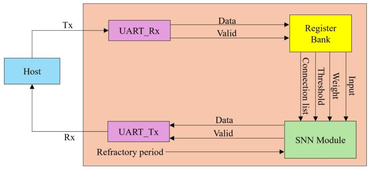
Neuromorphic Processor with Universal Interconnections Implemented on FPGA Enables Real-Time Inference and Experimentation (Quantum Zeitgeist) (9 mins)
Neuromorphic Chips: Could Memory Chips Make Relationships With Humanoids a Reality? (SK hynix) (11 mins)
Neuromorphic Chip Market to Reach USD 2.3 Billion by 2034 (openPR) (5 mins)
💥 Data Centers
Liquid cooling: the future of data center architecture and operations (Data Center Dynamics) (10 mins)
Data center cooling market surges to USD 34.12 billion by 2033, propelled by 10.3% CAGR (PR Newswire) (4 mins)
☁️ Cloud
AWS re:Invent 2025: How the industrial cloud is becoming physical (ARC Advisory Group) (13 mins)
Dec 2025: What’s new with Google Data Cloud (Google Cloud) (5 mins)
📡 Networking
Configuring data center networks with confidence (Nokia) (7 mins)
Funding News
Last week’s rounds covered a mid-sized set of deals across quantum, neuromorphic, semiconductors, and data centers, with a wide spread in deal sizes, ranging from €2M to $475M. The $25M Series A1 for Corintis is included here as well, as we missed it in last week’s overview.
Amount | Name | Round | Category |
|---|---|---|---|
€2M | Quantum | ||
$25M | Data Centers | ||
$25M | Neuromorphic | ||
$26M | Semiconductors | ||
$60M | Quantum | ||
$100M | Quantum | ||
$475M | Neuromorphic |
Bonus: Technologies unveiled at IEDM 2025 in San Francisco
The IEEE International Electron Devices Meeting (IEDM) took place this week in San Francisco, with a strong focus on advanced logic, AI efficiency, memory technologies, quantum devices, thin-film transistors, and silicon photonics. Selected highlights include:
HBM-on-GPU thermals: imec showed that co-optimization and system-level thermal mitigation can significantly reduce peak GPU temperatures under realistic AI training workloads.
Monolithic 3D integration: CEA-Leti’s FAMES Pilot Line demonstrated fully functional 2.5 V SOI CMOS devices fabricated at 400 °C, addressing a key constraint for large-scale 3D sequential integration.
Compute-in-memory devices: Georgia Tech and TSMC presented monolithic 3D capacitive memory architectures targeting compute-in-memory.
Beyond-CMOS and RF platforms: Progress was reported on 2D-material devices through collaborations involving TSMC, imec, and Intel, alongside AlN-based high-frequency transistors by NTT.
HBM packaging standards: JEDEC is developing the SPHBM4 specification, which reuses HBM4 DRAM dies but replaces the silicon interposer with an interface base die compatible with standard organic substrates, targeting equivalent bandwidth via 512 data signals and 4:1 serialization.
Automotive AI compute: Rivian announced an in-house 5 nm processor designed for vision-centric physical AI based on an Arm Cortex-A720AE v9 CPU, alongside an autonomy platform built around an end-to-end training data loop.


