Happy Monday! Here’s what’s inside this week’s newsletter:
Deep dive: The second part of our Memory Wall series takes a closer look at HBM (High Bandwidth Memory), explaining how HBM’s layered architecture, production process, and shifting market demand define its position in today’s high-performance memory landscape.
Spotlights: Q.ANT introduces its second-generation photonic Native Processing Unit for energy-efficient AI and HPC and d-Matrix partners with Alchip on a 3D DRAM-based inference accelerator that validates its in-memory compute approach on test silicon.
Headlines: Semiconductor updates from metrology to PCB and SRAM advances, expanding quantum–HPC integrations and defense strategies, progress in photonic pilots and acquisitions, neuromorphic sensing research, and large data center, networking, and AI build-outs and partnerships.
Readings: Semiconductor supply chain and packaging challenges, quantum error correction and simulation progress, renewed photonics investment, neuromorphic advances, and energy and sovereignty issues in data center and cloud infrastructure.
Funding news: A very active week with numerous Seed and Series A rounds across cloud, semiconductors, photonics, quantum, and data centers, while Lambda’s $1.5B Series E shows how a single large cloud round can dominate overall capital deployed.
Bonus: Washington’s latest semiconductor and AI moves, from slowing broad chip-import tariffs and approving controlled Nvidia Blackwell exports to the Gulf, to proposing SEMI Act tax credits and preparing new limits on state-level AI rules amid strong public support for AI safety.
Deep Dive: Breaking the Memory Wall Pt. 2 - A Closer Look at HBM (High Bandwidth Memory)
Building on last week’s analysis of FMC and Majestic Labs and their innovations in the memory stack, this issue turns to the memory technology at the core of all major AI accelerators: High Bandwidth Memory (HBM).
What is HBM
As outlined last week, each memory tier comes with its own trade-offs. SRAM provides high speed but offers very little density, while DRAM delivers high density but does not provide the bandwidth required for modern workloads.
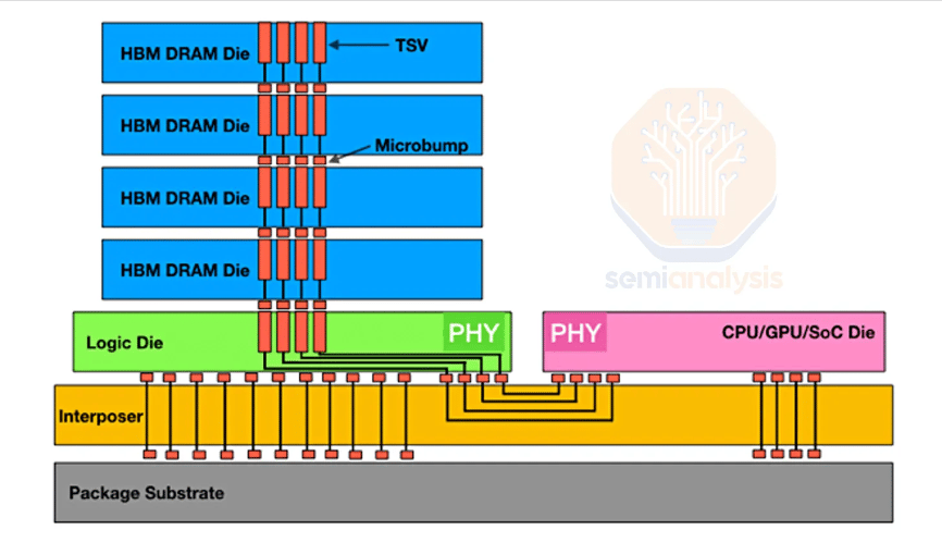
The dominant choice today is on-package High Bandwidth Memory (HBM), which combines vertically stacked DRAM layers, very wide data interfaces, and integration on the same package as the compute die. Because it is positioned directly beside GPUs, TPUs, and custom AI processors, HBM functions as the closest and fastest external memory layer available to these devices. Taken together, these design features allow HBM to provide a balanced mix of capacity, bandwidth, and efficiency compared to other memory types.
Hence, HBM is a memory technology that delivers:
high bandwidth through thousands of I/O connections
high density through vertically stacked DRAM dies
low energy per bit moved through very short transfer distances
This combination enables the multi-terabyte bandwidth required by current accelerators.
HBM Manufacturing
HBM production spans two main process stages:
Front-end processing: converting standard DRAM wafers into HBM wafers by forming TSVs (vertical connections through the silicon) and adding bumps (solder contacts for die-to-die connection) on both sides of the die.
Back-end processing: assembling and packaging the stacked dies using flows that support efficient joint formation, manage heat dissipation, and limit warpage and bump stress.
Two cross-cutting topics shape the overall manufacturing flow:
Yield challenges: arise from the demands of 3D stacking, delivering power through TSVs, and managing heat in a structure that becomes more sensitive as layer counts increase.
Bonding tools: must provide sub-micron alignment and controlled pressure to attach each die layer accurately, since misalignment or uneven force can damage bumps and reduce overall yield.
HBM Buyers and Demand
Demand for HBM has expanded rapidly in step with the growth of AI accelerators. Even with the increasing presence of custom ASICs, Nvidia is expected to remain the largest user of HBM in 2027. Its roadmap drives this, with Rubin Ultra alone moving to 1TB of HBM per GPU. Broadcom follows, supported by rising volumes of TPU and MTIA devices. Additional demand comes from OpenAI and SoftBank projects, which contribute smaller but still noticeable increases. Amazon is also becoming one of the major purchasers and follows a strategy of sourcing HBM directly rather than relying solely on design partners, which helps reduce its overall cost.
More detailed, chip-level bit forecasts are available in the Accelerator Model by SemiAnalysis.
Source: Scaling the Memory Wall: The Rise and Roadmap of HBM (SemiAnalysis)
Spotlights
⚡️ Q.ANT Unveils its Second-Generation Photonic Processor to Power the Next Wave of AI and HPC (Q.ANT)
“Q.ANT today announced the availability of its next-generation Native Processing Unit: The Q.ANT NPU 2, with enhanced nonlinear processing capabilities to deliver orders-of-magnitude gains in energy efficiency and performance for AI and high-performance workloads. By performing nonlinear mathematics natively in light, the Q.ANT NPU 2 enables entirely new classes of AI and scientific applications including physical AI and advanced robotics, next-generation computer vision and industrial intelligence, physics-based simulation and scientific discovery. Q.ANT is offering its NPUs directly as a 19” Server Solution including x86 host processor and Linux operating system.”
Stay tuned for our upcoming interview with Q.ANT on our blog!
🦾 d-Matrix and Alchip Announce Collaboration on World’s First 3D DRAM Solution to Supercharge AI Inference (d-Matrix)
“d-Matrix, the pioneer in generative AI inference for data centers, and Alchip, the high-performance and AI infrastructure ASIC leader, are collaboratively developing the world’s first 3D DRAM-based datacenter inference accelerator that will eliminate the performance and cost bottlenecks constraining today’s AI infrastructure.
The joint initiative combines Alchip’s ASIC design expertise with d-Matrix’s digital in-memory compute platform architecture. The collaboration has already enabled a key technology, d-Matrix 3DIMC™, that is featured on d-Matrix Pavehawk™ test silicon and has been successfully validated in d-Matrix’s labs.”
Headlines
Last week’s headlines featured new semiconductor updates, fresh quantum–HPC collaborations, progress in photonic and neuromorphic hardware, major data center expansion plans, and new alliances across networking and AI.
🦾 Semiconductors
Nearfield Instruments signs Multi-Year Development Project to Advance Semiconductor Metrology (Nearfield Instruments)
Advanced Memory Prices Likely to Double as DRAM Crunch Spreads on NVIDIA Pivot, Structural Factors (Counterpoint Research)
Synopsys Demonstrates Framework for Optimizing Manufacturing Processes with Digital Twins at Microsoft Ignite (Synopsys)
Nvidia’s record $57 billion revenue and upbeat forecast quiets AI bubble talk (TechCrunch)
⚛️ Quantum
Infleqtion and Oak Ridge National Laboratory Partner to Advance Quantum–HPC Integration (Infleqtion)
Supercomputing Centers to Integrate Quantum Processors Using NVIDIA’s NVQLink (The Quantum Insider)
NVIDIA and RIKEN Deploy New Supercomputers for AI and Quantum Research (The Quantum Insider)
Pentagon Elevates Quantum Tech to Core of Future Battlefield Strategy (The Quantum Insider)
QSolid Makes Prototype Quantum Computer Available for First External Testing (The Quantum Insider)
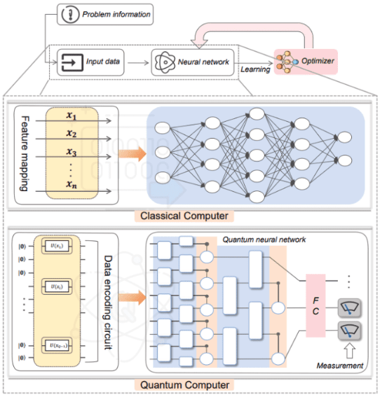
Qsentry Detects Quantum Neural Network Backdoors with 93.2% Accuracy, Even at 1% Poisoning Rates (Quantum Zeitgeist)
⚡️ Photonic / Optical
High Tech Campus Eindhoven to build cleanroom for TNO’s 6-inch photonic chip pilot line (Cleanroom Technology)
GlobalFoundries Acquires Advanced Micro Foundry, Accelerating Silicon Photonics Global Leadership and Expanding AI Infrastructure Portfolio (GlobalFoundries)
🧠 Neuromorphic
Two-dimensional MXene-based advanced sensors for neuromorphic computing intelligent application (EurekAlert!)
💥 Data Centers
500 MW data center campus in the works outside Leipzig, Germany (Data Center Dynamics)
📡 Networking
AWS claims cloud provider first with DWDM transponder (ComputerWeekly)
🤖 AI
Readings
This reading list covers semiconductor supply chain risks and packaging costs, quantum progress amid talent shortages, advances in photonic and neuromorphic chips, energy challenges in data centers, and Europe’s evolving stance on cloud sovereignty.
🦾 Semiconductors
New technologies and familiar challenges could make semiconductor supply chains more fragile (Deloitte) (9 mins)
Microcontrollers enter a new growth cycle as the market targets US $34 billion in 2030 (Yole Group) (9 mins)
Made in China 2025: Evaluating China’s Performance (U.S.-China Economic and Security Review Commission) (Page 5 to 8 - 14 mins)
The Thermal Trap: How Dielectrics Limit Device Performance (SemiEngineering) (24 mins)
New Panel Production Efforts Target Interposer Costs (SemiEngineering) (22 mins)
Issues In Ramping Advanced Packaging (SemiEngineering) (11 mins – Video)
⚛️ Quantum
Report: Error Correction Becomes Universal Priority But Talent Shortage Looms (The Quantum Insider) (8 mins)
Unprecedented Perlmutter Simulation Details Quantum Chip (Lawrence Berkeley Lab) (16 mins)
Google AI Outlines Path to Useful Quantum Applications (Quantum Zeitgeist) (32 mins)
Quantum-enhanced performance: Two-dimensional superconducting interference arrays overcome area limitations (Quantum Zeitgeist) (11 mins)
Real-space Time-Dependent Schrödinger Equation Solved with Fermionic Antisymmetric Spatio-Temporal Network (Quantum Zeitgeist) (12 mins)
⚡️ Photonic / Optical
Photonic edge intelligence chip for multi-modal sensing, inference and learning (Nature Communications) (53 mins)
Mode-locking in a semiconductor photonic bandgap laser (Communications Physics) (53 mins)
Reconfigurable chalcogenide integrated nonlinear photonics (Nature Communications) (67 mins)
Sustainable Photonics Manufacturing (AZO Optics) (6 mins)
How small can optical computers get? Scaling laws reveal new strategies (TechXplore) (6 mins)
🧠 Neuromorphic
Neuromorphic computing paradigms enhance robustness through spiking neural networks (Nature Communications) (54 mins)
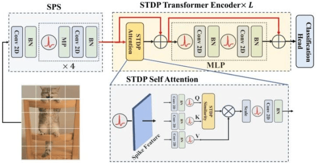
Spiking Neuromorphic Transformer Achieves Attention Via Synaptic Plasticity, Reducing Energy Costs Beyond 0.49 (Quantum Zeitgeist) (7 mins)
💥 Data Centers
In focus: Data centres – an energy-hungry challenge (European Commission) (4 mins)
☁️ Cloud
Sovereignty 2.0: Why Europe’s €180 million cloud bet matters (World Economic Forum) (16 mins)
🤖 AI
One Giant Leap for AI Physics: NVIDIA Apollo Unveiled as Open Model Family for Scientific Simulation (NVIDIA) (3 mins)
Funding News
Last week saw a very high number of rounds across the computing stack, with unusually dense activity at the Seed and Series A stages. Despite the large number of early-stage raises, overall capital was dominated by a single very large cloud round (Lambda’s $1.5B Series E).
Amount | Name | Round | Category |
|---|---|---|---|
CHF150K | Quantum | ||
$4.2M | Cloud | ||
$5.3M | Semiconductors | ||
$10M | Data Centers | ||
$12M | Photonics | ||
$13.6M | Cloud | ||
€14.1M | Semiconductors | ||
€16M | Photonics | ||
$25M | Semiconductors | ||
$34M | Cloud | ||
$80M | Data Center | ||
$140M | Photonics | ||
$1.5B | Cloud |
Bonus: U.S. Policy Signals for Chips and AI
This week brought several policy moves in Washington that shape both the chip industry and the broader AI landscape.
The administration is expected to slow down its plan for broad semiconductor-import tariffs, as officials assess whether the move could heighten tensions with China.
The U.S. also approved controlled exports of up to 35,000 NVIDIA Blackwell chips to the UAE and Saudi Arabia, subject to strict security and reporting requirements.
Statement on UAE and Saudi Chip Exports (U.S. Department of Commerce)
In Congress, the SEMI Investment Act was introduced to extend the 35% advanced manufacturing tax credit to U.S. producers of semiconductor materials, including substrates, thin films, and process chemicals.
Fitzpatrick, Boyle Launch Bipartisan SEMI Act to Reassert U.S. Control Over Critical Chip Materials and Strengthen American Manufacturing (U.S. House of Representatives)
At the same time, the White House is preparing an executive order aimed at limiting state-level AI regulation, even as a national poll shows that 80% of U.S. adults support maintaining federal rules focused on AI safety and data security.


